(China (Mainland))

Product Summary
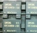
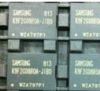
K9F2G08R0A - FLASH MEMORY - Samsung semiconductor
Features
Voltage Supply
- 1.65V ~ 1.95V
- 2.70V ~ 3.60V
? Organization
- Memory Cell Array : (256M + 8M) x 8bit
- Data Register : (2K + 64) x 8bit
? Automatic Program and Erase
- Page Program : (2K + 64)Byte
- Block Erase : (128K + 4K)Byte
? Page Read Operation
- Page Size : (2K + 64)Byte
- Random Read : 25μs(Max.)
- Serial Access : 25ns(Min.)
(*K9F2G08R0A: tRC = 42ns(Min))
256M x 8 Bit NAND Flash Memory
? Fast Write Cycle Time
- Page Program time : 200μs(Typ.)
- Block Erase Time : 1.5ms(Typ.)
? Command/Address/Data Multiplexed I/O Port
? Hardware Data Protection
- Program/Erase Lockout During Power Transitions
? Reliable CMOS Floating-Gate Technology
-Endurance : 100K Program/Erase Cycles(with 1bit/512Byte
ECC)
- Data Retention : 10 Years
? Command Driven Operation
? Intelligent Copy-Back with internal 1bit/528Byte EDC
? Unique ID for Copyright Protection
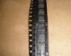
? Package :
- K9F2G08R0A-JCB0/JIB0 : Pb-FREE PACKAGE
63 - Ball FBGA I (10 x 13 / 0.8 mm pitch)
- K9F2G08U0A-PCB0/PIB0 : Pb-FREE PACKAGE
48 - Pin TSOP I (12 x 20 / 0.5 mm pitch)
- K9F2G08U0A-ICB0/IIB0
52 - Pin ULGA (12 x 17 / 1.00 mm pitch)
Diagrams