(China (Mainland))

Product Summary
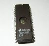
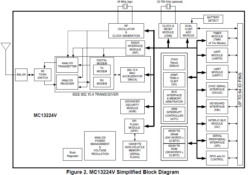
The MC13224V is Freescale third-generation ZigBee platform which incorporate a complete, low power, 2.4 GHz radio frequency transceiver, 32-bit ARM7 core based MCU, hardware acceleration for both the IEEE 802.15.4 MAC and AES security, and a full set of MCU peripherals into a 99-pin LGA Platform-in-Package (PiP).The MC13224V solution can be used for wireless applications ranging from simple proprietary point-to-point connectivity to complete ZigBee mesh networking. The MC13224V is designed to provide a highly integrated, total solution, with premier processing capabilities and very low power consumption.
Parametrics
MC13224V absolute maximum ratings: (1)Maximum Junction Temperature TJ: 125 °C; (2)Storage Temperature Range Tstg: -55 to 125 °C; (3)Moisture Sensitivity Level: MSL3-260; (4)Reflow Soldering Temperature (for reflow soldering profile and other LGA module reference information, see Freescale application note, AN3311): 250 °C; (5)Power Supply Voltage VBATT, VDDINT: -0.3 to 3.7 Vdc; (6)Digital Input Voltage Vin: -0.3 to (VDDINT + 0.2) Vdc; (7)RF Input Power Pmax: 10 dBm; (8)Instantaneous Maximum Current (Single Pin Limit) ID: ± TBD mA.
Features
MC13224V features: (1)IEEE 802.15.4 standard compliant on-chip transceiver/modem: 2.4 GHz ISM Band operation; 16 selectable channels; Programmable transmitter output power (-30 dBm to +4 dBm typical); World-class receiver sensitivity; < -96 dBm typical receiver sensitivity using DCD mode (<1% PER, 20-byte packets); < -100 dBm typical receiver sensitivity using NCD mode (<1% PER, 20-byte packets); (2) Supports standard IEEE 802.15.4 signaling with 250 kbps data rate; (3)32-bit ARM7TDMI-S CPU core with programmable performance up to 26 MHz (24 MHz typical); (4)Extensive on-board memory resources: 128 Kbyte serial FLASH memory (will be mirrored into RAM); 96 Kbyte SRAM; 80 Kbyte ROM; (5)Best-in-class power dissipation: 21mA typical RX current draw (DCD mode) with radio and MCU active; 28 mA typical TX current draw with radio and MCU active (coin cell capable); 5mA maximum current draw with MCU active (radio off); 0.9mA maximum current with MCU idle (radio off); 1.1 μ maximum Hibernate current (retain 8 Kbyte SRAM contents); 0.3μ maximum Off current (device in reset); (6)Extensive sleep mode control and variation: Hibernate and Doze low power modes; Programmable degree of power down; Clock management; Onboard 2kHz oscillator for wake-up timer; Optional 32.768 kHz crystal oscillator for accurate real-time sleep mode timing and wake-up with a possible sleep period greater than 36.4 hours; Wake-up through programmable timer, external real-time interrupts, or ADC timer; (7)Extensive MCU peripherals set: Dedicated 802.15.4 modem/radio interface module (RIF); Dedicated NVM SPI interface for managing FLASH memory; Two dedicated UART modules capable of 2Mbps with CTS/RTS support; SPI port with programmable master and slave operation; 8-pin keyboard interface (KBI) supports up to a 4x4 matrix. Also, provides up to 4 asynchronous interrupt inputs for wake-up; Two 12-bit analog-to-digital converters (ADCs) share 8 input channels; Four independent 16-bit timers with PWM capability. These can cascade in combinations up to 64-bit operation; Inter-integrated circuit (I2C) interface; Synchronous Serial Interface (SSI) with I2S and SPI capability and FIFO data buffering; Up to 64 programmable I/O shared by peripherals and GPIO; (8)Powerful In-circuit debug and FLASH programming available via on-chip debug ports: JTAG debug port; Nexus extended feature debug port; (9)System protection features: Low battery detect; Watchdog timer (COP); Sleep mode timer; (10)Low external component count: Only antenna needed for single-ended 50-?RF interface (balun in package); Only a single crystal is required for the main oscillator; programmable crystal load capacitors are on-chip; All bypass capacitors in package; (11)Supports single crystal reference clock source (typical 24 MHz crystal with 13 - 26 MHz usable) with on-chip programmable crystal load capacitance or external frequency source. Also provides; (12)onboard 2kHz oscillator for wake-up timing or an optional 32.768 kHz crystal for accurate low power timing.; (13)2.0V to 3.6V operating voltage with on-chip voltage regulators; down to 1.8V with off-chip regulation; (14)Optional buck converter for better battery life.; (15)-40℃ to +105℃ temperature range; (16)RoHS-compliant 9.5mm x 9.5mm x 1.2mm 99-pin LGA package.
Diagrams
| Image | Part No | Mfg | Description |  |
Pricing (USD) |
Quantity | ||||||||||||
|---|---|---|---|---|---|---|---|---|---|---|---|---|---|---|---|---|---|---|
 |
 MC13224V |
Freescale Semiconductor |
RF Transceiver PIP 802.15.4 2.4G IND |
Data Sheet |
|
|
||||||||||||
|
MC13224VR2 |
Freescale Semiconductor |
RF Transceiver PIP 802.15.4 2.4G IND |
Data Sheet |
|
|
||||||||||||